PhaseBlue® Series Circuit Materials:
Lightweight, Flexible PCB Solutions for High-Speed, High-Frequency, Reliable Communications
PCBs: A Mainstay of the Modern World
While the concept of a printed circuit board (PCB) has been known since the early 1900s when Albert Hanson described flat foil conductors laminated to an insulating board in multiple layers within telephone exchange systems, it wasn’t until the 1930s that Paul Eisler used the first PCB within a radio, leading to three ground-breaking patents: 639111 (Three-Dimensional Printed Circuits), 639178 (Foil Technique of Printed Circuits), and 639179 (Powder Printing). In the 1950s copper clad laminates (CCLs) were developed, with the first method for plating a uniform layer of copper onto an aperture PCB patented by the Bunker Ramo Corporation in 1968. This paved the way for production of PCBs in high volumes and arguably contributed to the rapid rise in electronic applications seen over the last 60 years or so.
Today’s state-of-the-art is significantly more advanced than early designs, but the fundamental aspects that drive PCB materials innovation have remained the same: namely, the microstructure of the copper laminate layer and the substrate. While the quality and method through which copper is laid onto the substrate are important – with common techniques including laminating and electrodeposition – and can impact upon the downstream processing operations, it’s the substrate itself that has the largest impact upon PCB performance.
More specifically, it’s the substrate’s physical properties that matter. In particular, both the dielectric constant (Dk) and dissipation factor (Df) play a critical role in PCB performance.
Dk describes how a material influences signal propagation speed. Lower Dk values allow electromagnetic signals to travel faster, improving transmission efficiency.
Df measures energy losses in the material, typically from dipole rotation within the organic substrate. Lower Df values correspond to reduced conversion of signal energy into heat, resulting in lower losses and better signal integrity.
At low frequencies, such as in audio circuits, power supplies, and control systems, limitations in Dk and Df can usually be managed without difficulty. At higher frequencies, however, precise optimization of these parameters is critical to ensure efficiency, reliability, and speed.
Drawbacks of PTFE-Based Substrates
Perfluorinated substrates (PTFE-based) have been the market leaders in high-frequency PCB design and manufacture for decades. Their low dielectric constant (Dk) values and excellent dissipation factor
(Df) performance drove rapid adoption across the industry. However, several significant drawbacks limit their long-term viability.
Dielectric Instability: PTFE-based substrates typically undergo a conformational change in the polymer chains at, or near, room temperature, altering dielectric properties and negatively impacting both Dk and Df. Structural modifications, such as incorporating ceramic fillers or reinforcing fibers, can improve processibility. However, these often raise the Dk value, slowing signal transmission, decreasing efficiency, and reducing flexibility and diminishing Df performance.
Thermal and Chemical Limitations: PFAS-based materials start to decompose at 260 °C, weakening the substrate structure and introducing potential failure points. Decomposition can also release toxic hydrogen fluoride (HF), creating additional safety and environmental concerns.
Bonding Challenges: With inherently low surface energy and a slippery nature, PTFE substrates are notoriously difficult to bond reliably with other materials, complicating manufacturing processes.
Regulatory Pressures: Impending restrictions on the use of perfluorinated materials in both the US and EU are further accelerating the search for PTFE alternatives. Electronics manufacturers are increasingly prioritizing high-performing, PFAS-free substrates that meet both technical and regulatory demand.
PhaseBlue Series Circuit Materials
A PFAS-free polyimide-based dielectric substrate
PhaseBlue® Series Circuit Materials are innovative laminates engineered with a proprietary nanoporous polyimide core composed of 85% air and 15% organic polyimide. This aerogel-enabled core outperforms traditional PTFE-based PCBs across multiple metrics (see Table 1).
As a fluorine-free, U.S.-designed material, PhaseBlue® products not only address the growing environmental concerns surrounding PFAS and polyhalogenated materials, but also ensure full compliance with IPC-4202C.
Constant Dk values and Tg properties
With an exceptionally low Dk of 1.3 – 1.5 at 1 GHz, which remains constant across a frequency range of 1 to 10 GHz, and Tg of 305 °C, significantly higher than most PTFE-based materials, PhaseBlue materials exhibit impressive thermal stability during processing and operational activities. Importantly, the ‘dielectric knee’, a common drawback of perfluorinated substrates, is not seen under high temperatures.
| Property | PhaseBlue® | PTFE |
| PFAS-based | No | Yes |
| Dk, 1.0 GHz | 1.3 – 1.5 | 2.1 |
| Df, 1.0 GHz | < 0.001 | < 0.001 |
| Dielectric knee temperature, °C | Not observed | 19 – 25 |
| Density, g/cm3 | < 0.45 | 2.2 |
| Tg, °C | 305 | 120 – 143 |
| Surface energy, dyne/cm | > 60 | 19 |
Lightweight and flexible
As well as superior Dk and Df behaviors when compared with the market leaders, PhaseBlue® maintains flexibility under a range of conditions enabling facile application across topologically uneven surfaces. Finally, the nanoporous structure means that PhaseBlue® materials have a density of < 0.45 g/cm3, lower than that of leading competitors, rendering them ultra-lightweight.
PhaseBlue Series Circuit Materials: A leader in PCBs for High-Frequency Application
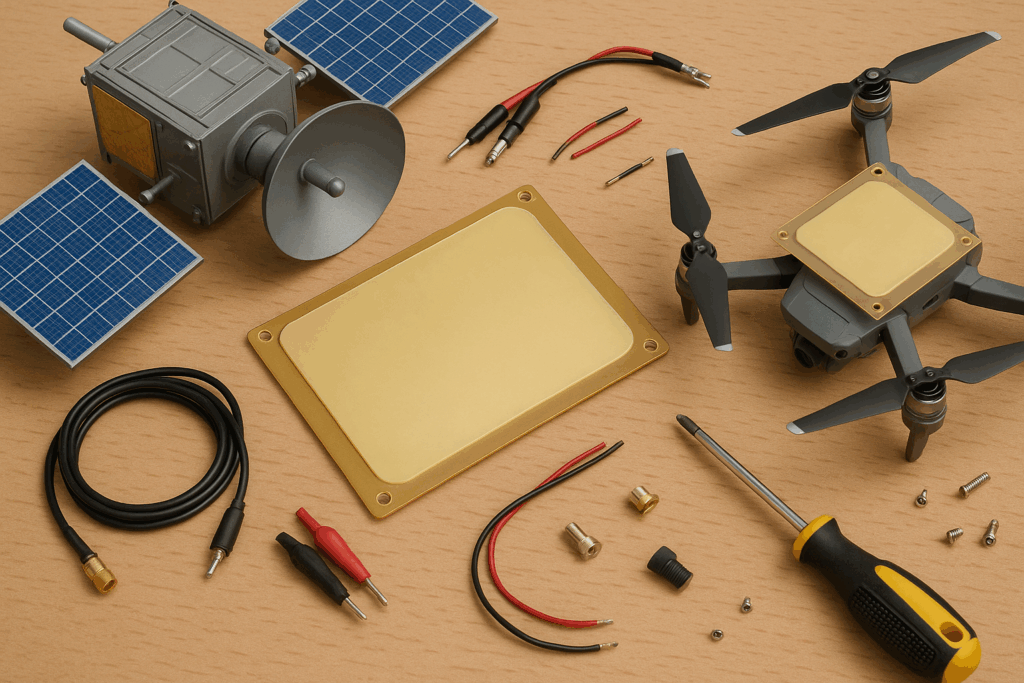
Designed specifically for high-frequency PCB applications, PhaseBlue®-based substrates provide measurable improvements in Dk, Df, weight, and flexibility relative to current industry state-of-the-art, offering clear operational advantages and out performing competitors across several key technical areas. Specifically designed to comply with slash sheet IPC-4202C, this US-designed and made PCB material has application across a range of communication devices, including patch and phased-array antennas and radomes, CubeSats and small satellites, UAV antennas, aerospace and high-speed communications.
To learn more about this newest addition of products, visit the site page: https://www.blueshiftmaterials.com/phaseblue-series-circuit-materials/
Or download the:
- Technical Product Brief: https://www.blueshiftmaterials.com/wp-content/uploads/2025/09/Tech-Product-Brief.pdf
- Technical Data Sheet: https://www.blueshiftmaterials.com/wp-content/uploads/2025/09/PhaseBlue-SCM-TDS.pdf
- Design Guide: https://www.blueshiftmaterials.com/wp-content/uploads/2025/09/PhaseBlue-Design-Guide.pdf
- Processing Guide: https://www.blueshiftmaterials.com/wp-content/uploads/2025/09/PhaseBlue-Processing-Guide.pdf
- One-Page Overview: https://www.blueshiftmaterials.com/wp-content/uploads/2025/09/One-Page-Overview.pdf