PhaseBlue:
Lighter. Smarter. Design‑ready.
PFAS‑Free & Halogen‑Free
Sustainably compliant materials that meet modern environmental standards.
Up to 80% Lighter
Significant weight savings versus traditional laminates for mass‑critical designs.
Ultra‑Low Dk / Df
Stable dielectric performance across wide frequencies to reduce signal loss.
High‑Temp Survivability
Reliable beyond PTFE operating limits for harsh environments.
Excellent Formability
Flexible, formable structure enables tight bends and 3D shapes.
FR‑4 Process Compatible
Works with standard DES, etchback, drilling and plating workflows.
State-of-the-Industry
High‑Frequency Signal Loss
As data rates increase, traditional laminates exhibit attenuation and dielectric losses. Designers need ultra‑low Dk and Df to maintain signal integrity in 5G, mmWave, and high‑speed digital applications.
High‑Temperature Limitations
Dense multi‑layer boards and high‑power components stress conventional CCLs. Our material delivers superior high‑temperature stability—outperforming PTFE—for long‑term durability and reliability under extreme conditions.
Rigid & Bulky Substrates Limit Design Freedom
Traditional rigid substrates add weight and constrain layout. PhaseBlue® combines ultralight construction with exceptional flexibility for tighter bend radii, thinner form factors, and creative 3D geometries.
100% Sustainably Compliant
- Stable Dk across wide frequency range
- Easy flex & rigid‑flex PCB integration
80% Weight Savings
-
High‑Temp survivability well beyond PTFE
-
IPC‑4202/15 compliant • Made in the USA
*Formulated without intentionally added per- and polyfluoroalkyl substances; claim based on composition and aligned with FTC Green Guides and Green Science Policy Institute PFAS-Free criteria.
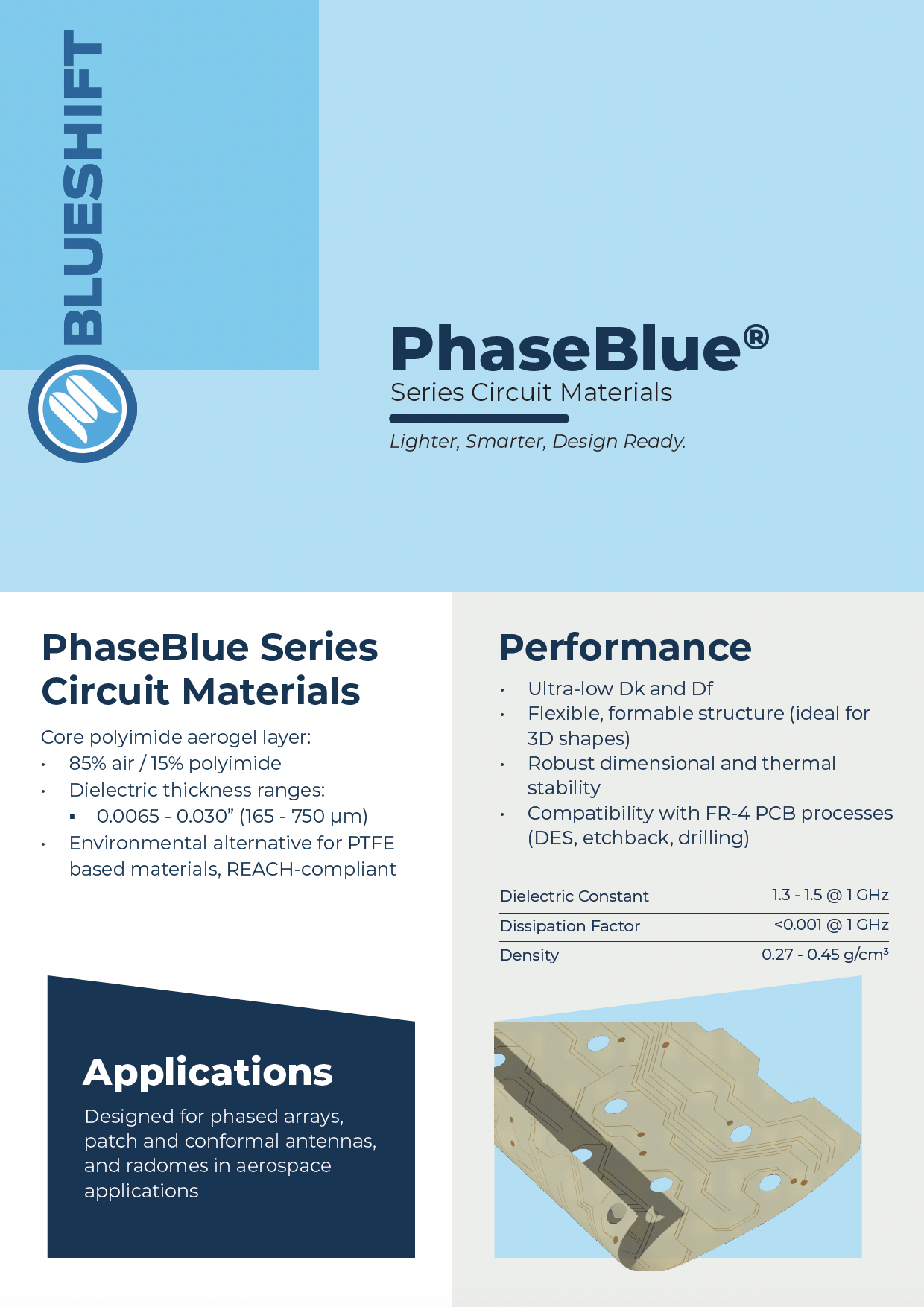
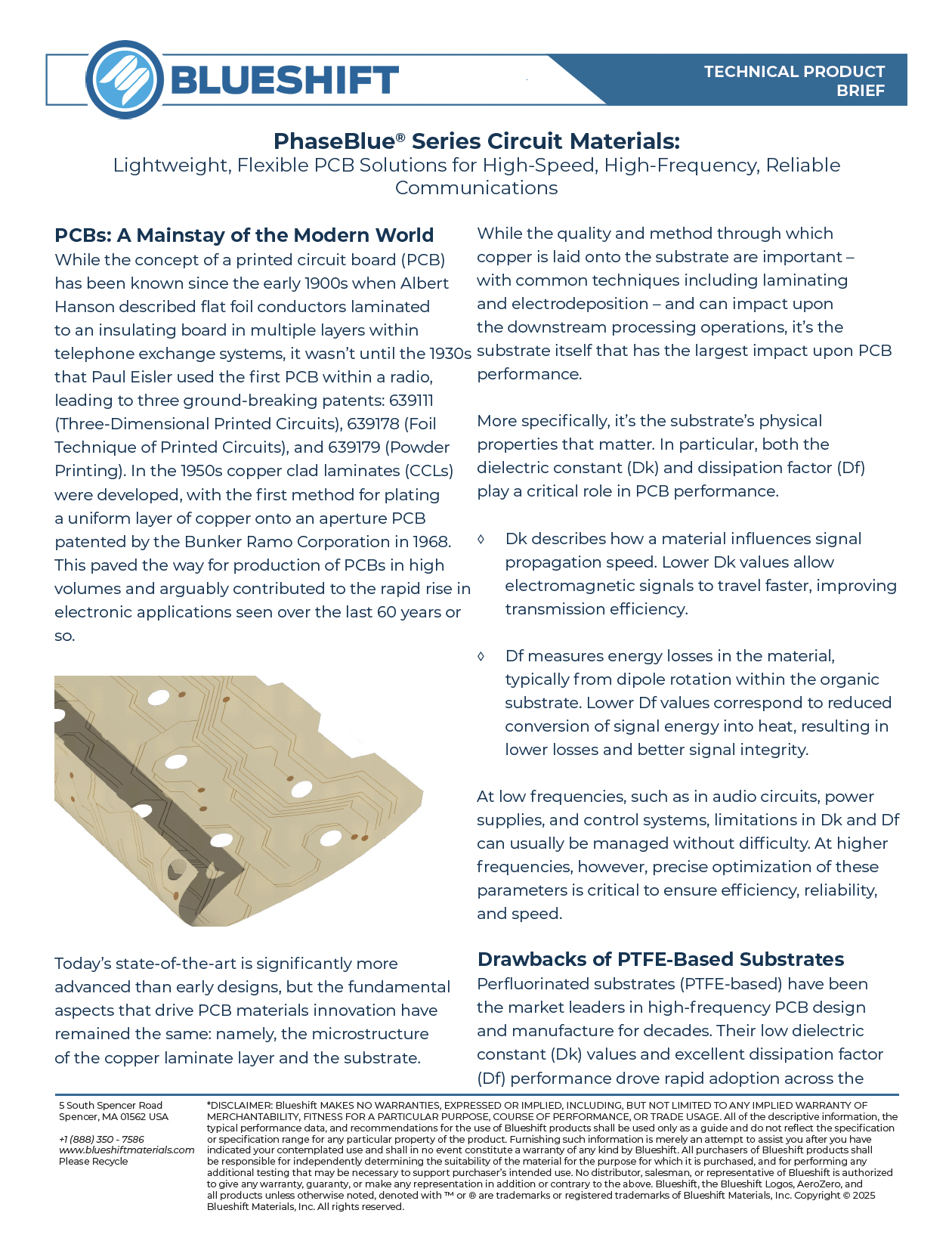
Core Technology
Density
- 0.27 – 0.45 g/cm³
Dielectric Constant (Dk) @ 1 GHz
- 1.3 – 1.5
Core Polyimide Aerogel Composition
- 85% air / 15% polyimide
Dissipation Factor (Df) @ 1 GHz
- < 0.001
Dielectric Thickness Range
- 0.0065 – 0.030 in (165 – 750 µm)
Compliance
- PFAS‑Free, Halogen‑Free, REACH‑Compliant, IPC‑4202/15
Applications
- Phased arrays
- Patch & conformal antennas
- Radomes
- Aerospace platforms
- mmWave, 5G & high‑speed digital systems
Processing Essentials
- Avoid plasma etchback—use gentler cleaning
- Monitor drill and plating quality
- Limit lamination pressures and temperatures
- Limit heat exposure during soldering (passes IPC solder float)
Handling & Storage
- Temperature: 70 ± 5 °F (21 ± 3 °C)
- Relative Humidity: below 50%
- Keep in original packaging with sulfur‑free paper
- Handle using rigid frames to avoid tears and deformation
Technical Data Sheet
Ready to build lighter, faster, and cooler?
Let’s talk PhaseBlue next-gen series circuit materials.